PARAMETERS OF A SOLAR CELL AND CHARACTERISTICS OF A PV PANEL
450W solar panel parameters
A 450w solar panel is designed to generate approximately 450 watts of electrical power under standard test conditions (STC). STC typically include a solar irradiance of 1000 W/m², a cell temperature of 25°C, and an air mass of 1.5. [pdf]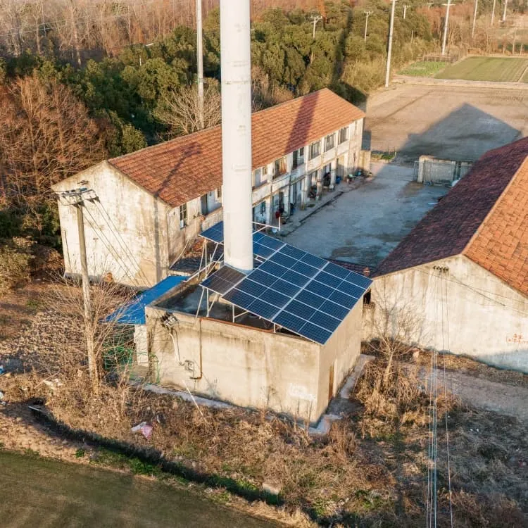
Solar cell panel photovoltaic power station
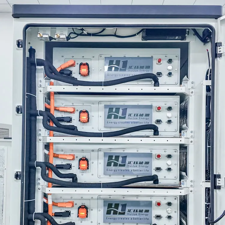
The solar power plant is also known as the Photovoltaic (PV) power plant. It is a large-scale PV plant designed to produce bulk electrical power from solar radiation. The solar power plant uses solar energy to produce electrical power. Therefore, it is a conventional power plant. Solar energy can be used directly to. . The major components of the solar photovoltaic system are listed below. 1. Photovoltaic (PV) panel 2. Inverter 3. Energy storage devices 4. Charge controller 5. System. . A solar cell is nothing but a PN junction. The plot of short-circuit current (ISC) and open-circuit voltage (VOC) describes the performance of the solar cell. This plot is shown in the figure. . The solar panels are classified into three major types; 1. Monocrystalline Solar Panels 2. Polycrystalline Solar Panels 3. Thin-film Solar. . The solar power plant is classified into two types according to the way load is connected. 1. Standalone system 2. Grid-connected system . Most solar parks are PV systems, also known as free-field solar power plants. They can either be fixed tilt or use a single axis or dual axis . While tracking improves the overall performance, it also increases the system's installation and maintenance cost. A converts the array's power output from to , and connection to the is made through a. [pdf]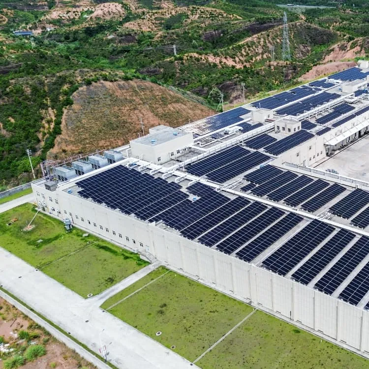
CdTe solar panel performance parameters
Two pivotal parameters are optimized to enhance CdTe cell performance: cell thickness, a key factor in augmenting performance and curtailing production costs, and doping density, a critical parameter for elevating open-circuit voltage and, in turn, cell performance. [pdf]FAQS about CdTe solar panel performance parameters
How effective is a CdTe solar cell?
When the thickness related to the newly developed CdTe PV cell is reduced by 0.5 μm, it obtains an overall effectiveness (ƞ) of 27.35%. This indicates a significant improvement in absorber layer effectiveness. This is primarily because of the solar cell’s 1 μm-thick CdTe and FeSi 2 layers serve as absorbers.
What is the difference between CDs and CdTe solar cells?
On the other hand, CdS has a bandgap energy of 2.42 eV, and transmits most of the visible spectrum . Thin film CdTe solar cells are typically hetero-junctions with CdS being the n-type partner, or window layer. The absorber layer thickness for thin film CdTe solar cells is normally between 2 and 10 μm .
How do CdTe solar panels compare to other solar panels?
How Do They Compare to Other Panels? The Cadmium Telluride (CdTe) solar technology was first introduced in 1972 when Bonnet and Rabenhorst designed the CdS/CdTe heterojunction that allowed the manufacturing of CdTe solar cells. At first, CdTe panels achieved a 6% efficiency, but the efficiency has tripled to this day.
What are the advantages of CdTe photovoltaic solar cells?
CdTe photovoltaic solar cells with single and double absorber layers of ultrathin layers have enhanced efficiencies and reduced costs. It is necessary to improve how these solar cells absorb light. Making the layer narrower can help to cut down on the amount of material required, as well as costs related to fabrication.
How to design a CdS/CdTe solar cell?
While designing a CdS/CdTe solar cell, a buffer layer of CdS (Eg = 2.45 eV) is mostly grown by CBD technique on a soda lime, ITO and FTO glass substrates, and the absorber layer of CdTe is deposited mainly by CSS technique [31, 32, 33, 34, 35]. Finally, a back contact is needed to complete the structure of a CdTe solar cell.
What is a typical CdTe/CdS solar cell structure?
A typical CdTe/CdS solar cell structure consists of the following four layers (Fig. 1): Schematics of a typical superstrate CdS/CdTe solar cell structure. 1. A front contact: Usually, it is a transparent conductive oxide layer. 2. A window layer: In most of the cases, it is a CdS thin film.